Microsoft unveils Maia 300 chip to cut reliance on Nvidia GPUs
Microsoft announces its third-generation Maia 300 AI chip, designed for efficient inference and agentic tasks, with production rollout starting in 2027.
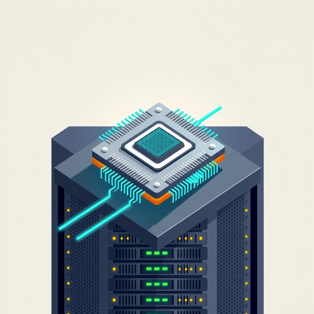
Microsoft has announced its third-generation in-house AI accelerator, the Maia 300, positioning it as the primary inference system for its cloud services. The company plans to begin rolling out the new silicon to production workloads in 2027, aiming to reduce dependence on external GPU suppliers like Nvidia and AMD while improving energy efficiency.
What happened
The Maia 300 is the successor to the Maia 200, which was announced earlier this year and is currently running production workloads for services such as Microsoft Copilot, GitHub Copilot, and Microsoft Foundry. Scott Guthrie, executive vice president of Microsoft’s cloud group, stated that the new chip is designed specifically for emerging AI demands, including long-context reasoning, latency-sensitive conversations, and sustained multi-step agentic tasks. The goal is to make Maia the core infrastructure for Microsoft’s AI products rather than relying primarily on third-party hardware.
Efficiency is the central metric for this generation. Microsoft expects the Maia 300 to deliver 40 percent more tokens per megawatt compared to leading GPU-based systems. In a full configuration using 96 accelerators, the company claims the rack-scale token throughput will be up to seven times higher than that of the Maia 200. These gains are intended to support multi-gigawatt deployments starting in 2027, allowing Microsoft to scale its Azure Maia family significantly.
This hardware strategy is tightly coupled with Microsoft’s broader AI ambitions. Mustafa Suleyman, CEO of Microsoft AI, emphasized the need for a platform that the company owns and co-designs with its models. By controlling the silicon layer, Microsoft aims to compete more effectively with rivals like Google DeepMind, OpenAI, and Anthropic. The move reflects a industry-wide trend where large tech firms develop custom silicon to optimize performance and cost for their specific model architectures.
How it works
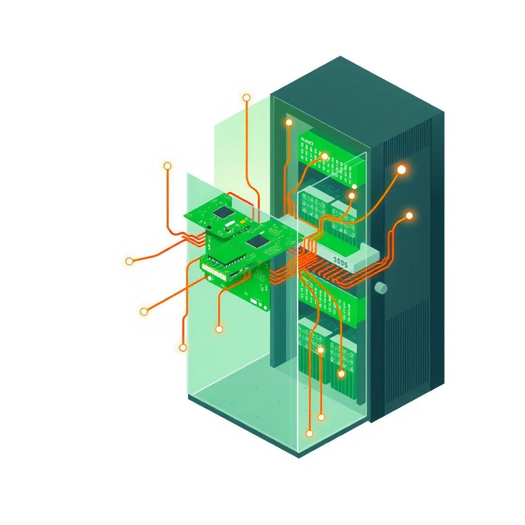
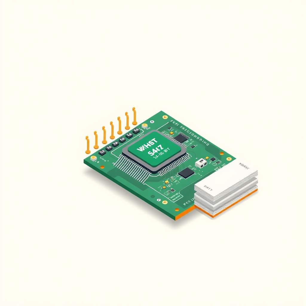
The Maia 300 achieves its efficiency improvements through a new chiplet architecture built on TSMC’s N2P process node. Unlike traditional monolithic designs, this approach separates compute, memory controller, and input/output functions into distinct components. This separation allows each function to utilize the manufacturing technology best suited for its specific role, thereby increasing the total silicon area dedicated to actual compute performance.
By decoupling these functions, the design reduces bottlenecks that often limit throughput in dense AI workloads. The architecture is optimized for the specific types of inference tasks that dominate modern AI usage, such as maintaining context over long conversations or executing complex, multi-step agent workflows. This hardware-software co-design ensures that the physical capabilities of the chip align closely with the operational requirements of Microsoft’s latest AI models.
Key details
- The Maia 300 will start being rolled out to production workloads in 2027.
- Microsoft expects 40 percent more tokens per megawatt compared to leading GPU-based systems.
- A 96-accelerator configuration delivers up to 7x the rack-scale token throughput of the Maia 200.
- The chip uses a chiplet architecture built on TSMC’s N2P process node.
- Compute, memory controller, and I/O functions are separated to optimize silicon area and technology usage.
- Maia 300 is designed for long-context reasoning, latency-sensitive conversations, and agentic tasks.
Why it matters
For software engineers and infrastructure leads, this shift signals a maturing ecosystem where custom silicon becomes the norm for large-scale AI deployment. Relying on general-purpose GPUs often means paying for capabilities that are not fully utilized or dealing with power constraints that limit scale. Custom accelerators like Maia 300 allow for tighter integration between the model architecture and the hardware, resulting in better cost-efficiency and performance per watt. This trend may encourage other major cloud providers to accelerate their own custom silicon roadmaps.
The focus on agentic tasks and long-context reasoning also highlights the changing nature of AI workloads. As applications move beyond simple query-response interactions to complex, multi-step processes, the underlying hardware must support sustained low-latency performance. Engineers building next-generation AI applications should anticipate that infrastructure providers will increasingly offer specialized tiers optimized for these specific workload types, rather than one-size-fits-all GPU instances.
What you can do
- Monitor the rollout timeline for Maia 300 on Azure to plan future infrastructure migrations.
- Evaluate current AI workloads to identify opportunities for long-context or agentic optimizations.
- Stay informed about TSMC’s N2P process node developments to understand broader industry efficiency trends.
- Consider how hardware-software co-design principles might apply to your own model deployment strategies.
- Review energy efficiency metrics when comparing cloud AI service providers for large-scale projects.
- Keep an eye on competitor announcements from Google, Amazon, and others regarding custom AI silicon.